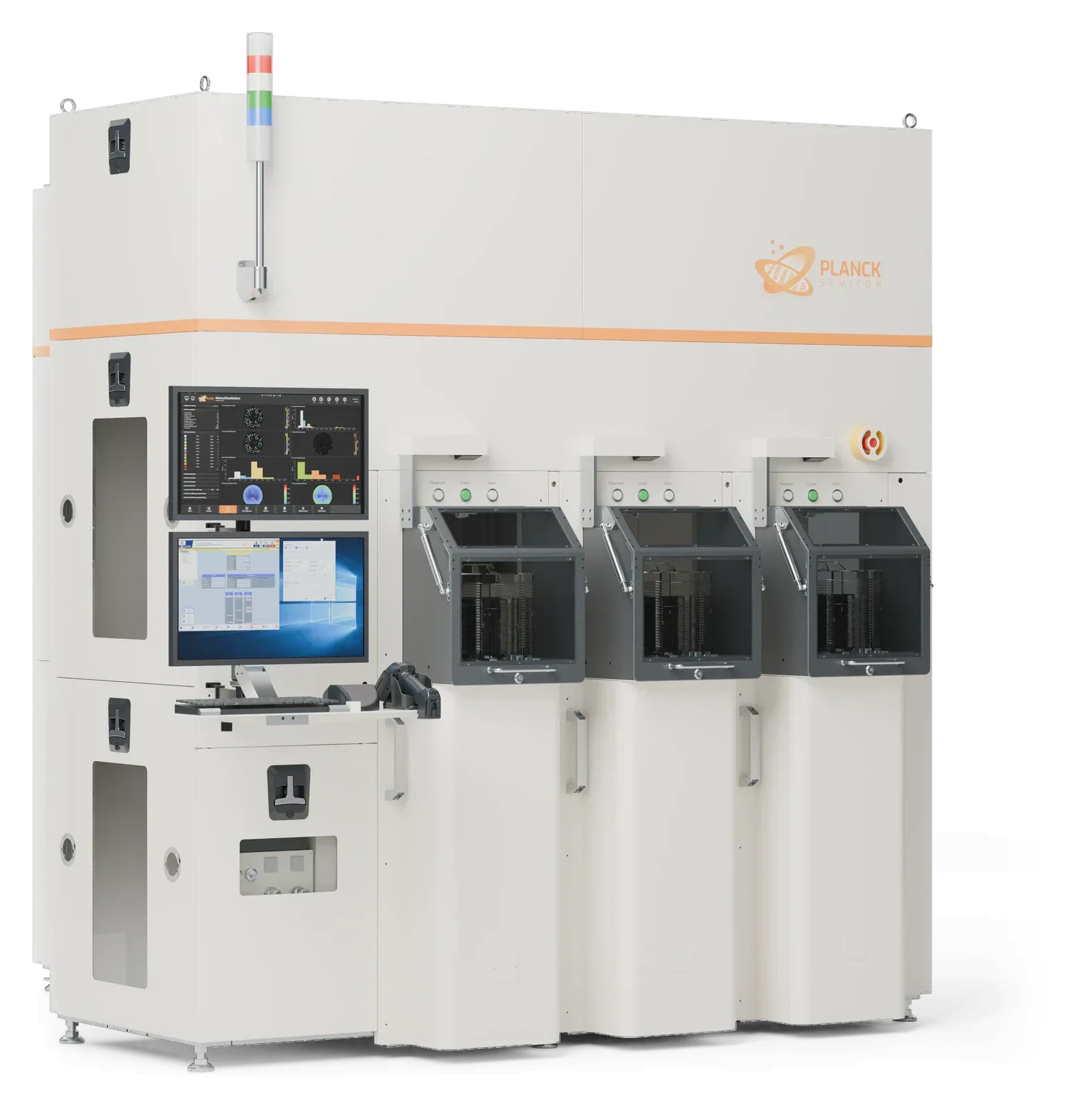
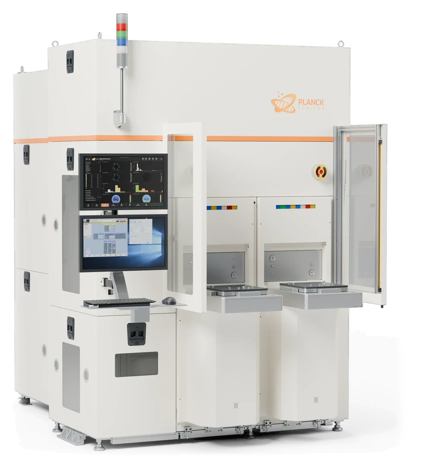
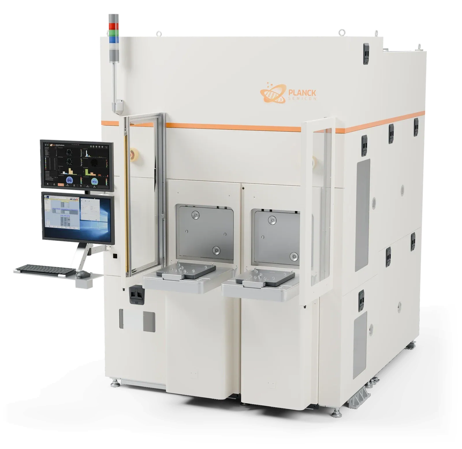
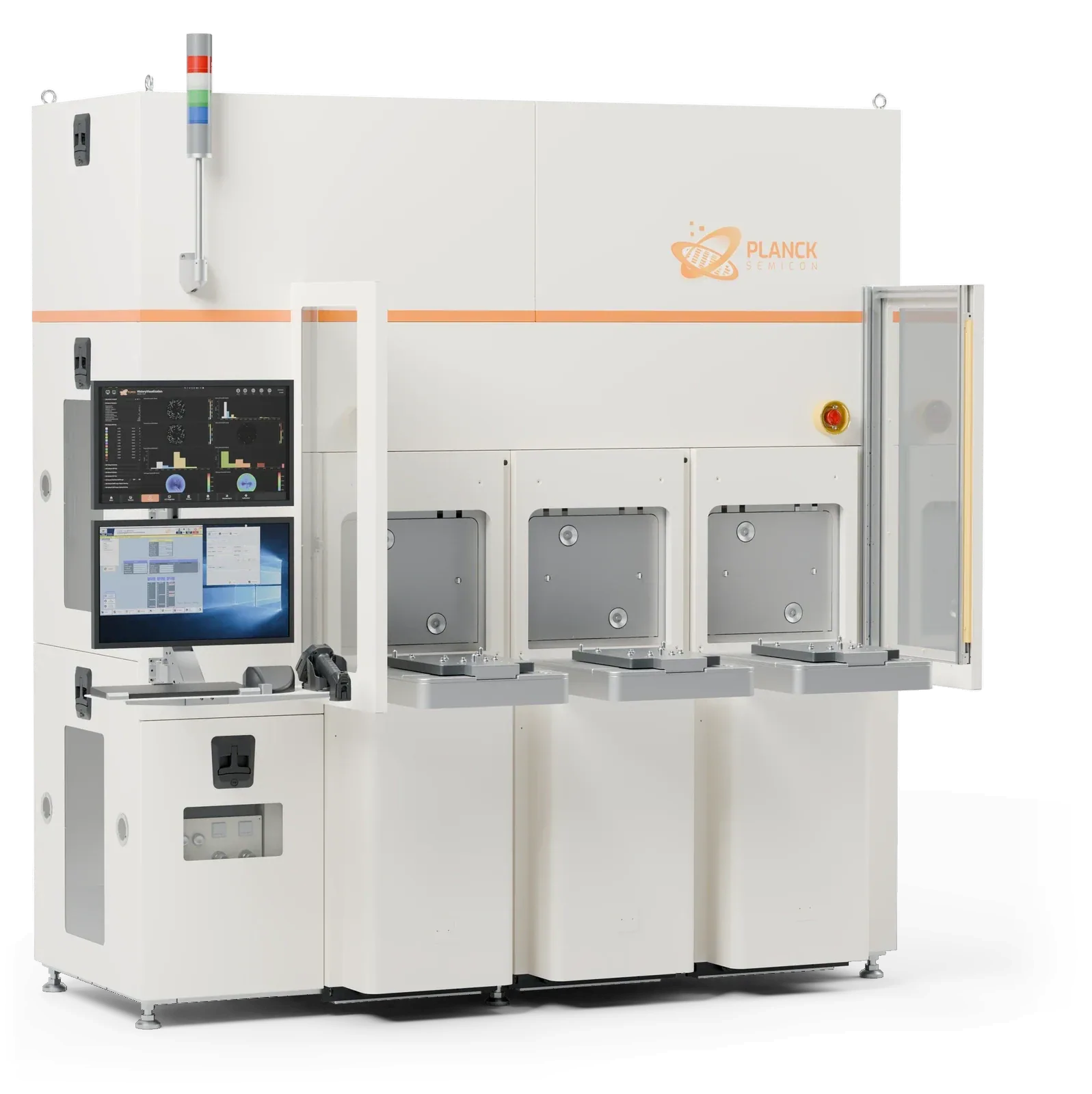
Inspection& metrology

Defect inspection, nano-topography and geometry metrology for front-end fabs, advanced packaging, power devices and compound semiconductors

Four application areasprocess control fromsubstrate to shipment

Choose your application area to see the platforms that serve it and the process steps they cover on the line

01 Front-End Fab · Logic and Memory

Focus

  • Incoming QC
  • Pre-litho backside and geometry control
  • Fast ADI
  • Defect and topography monitoring after etch, film and CMP
  • Tool cleanliness

02 Advanced Packaging · TSV, Hybrid Bonding, Glass Substrates

Focus

  • RDL and Bump pattern defects
  • TSV / TGV depth and CD
  • Bonding voids
  • Stack thickness
  • Warpage

03 Power Devices · IGBT and SiC MOSFET

Focus

  • Trench CD and depth
  • Thinned-backside topography
  • Backside particles
  • 100% patterned-wafer inspection

04 Compound Semiconductors & Silicon Substrates

Focus

  • SiC / GaN substrate and epi defects
  • Nano-topography
  • Particles
  • Wafer edge
  • Geometry sorting

No selectionSelect an area above to see its focus and the platforms that serve it

6 steps 9 platforms

Process steps × platform coverage

  • Main application
  • Optional or by configuration
Process stepInspection7Metrology2Platforms
KIBOUnpatternedACONCAPatternedCANIGOBacksideMUSHIWafer edgeCARPPAProcess controlVEYMONTNano-topographyDRAKENSSiC defectsNANSIMulti-channelELBRUSWafer geometry
Incoming Substrate and Wafer QC7
Epitaxy4
Lithography·Etch·Thin Film6
CMP·Thinning7
Advanced Packaging RDL Bump TSV·Bonding·Glass Substrate6
Outgoing QC·Tool and Process Cleanliness Monitoring7
Reach5 / 63 / 65 / 64 / 63 / 64 / 63 / 65 / 65 / 6
PlatformIncoming Substrate and Wafer QCEpitaxyLithography·Etch·Thin FilmCMP·ThinningAdvanced Packaging RDL Bump TSV·Bonding·Glass SubstrateOutgoing QC·Tool and Process Cleanliness MonitoringReach
Inspection7
KIBOUnpatterned5 / 6
ACONCAPatterned3 / 6
CANIGOBackside5 / 6
MUSHIWafer edge4 / 6
CARPPAProcess control3 / 6
VEYMONTNano-topography4 / 6
DRAKENSSiC defects3 / 6
Metrology2
NANSIMulti-channel5 / 6
ELBRUSWafer geometry5 / 6
Platforms746767

Nine platform seriesfor inspectionand metrology

09 SERIESINSPECTION 07METROLOGY 02

KIBO Series Unpatterned Wafer Defect Inspection System

01 / 09Inspection Systems

KIBO Series Unpatterned Wafer Defect Inspection System

KIBO Series

Unpatterned Wafer Defect Inspection System

Purity, proven

High-speed full-wafer scanning of bare silicon, epi, oxide, nitride and metal surfaces, with particles, scratches and haze counted, located and classified automatically and sensitivity from the μm range down to 1x nm

  • Unpatterned wafer
  • Particle inspection
Top particle sensitivity
1x nm
Spot-scan and line-scan models from the μm range down to 1x nm
Transparent and opaque alike
Any substrate
Si, SiC, GaN, sapphire, glass
Count · Locate · Bin
Auto-classify
Particles, scratches, haze, Wafer Map output

View details

02 / 09Inspection Systems

ACONCA Series Fully Automatic Patterned Wafer Optical Inspection System

ACONCA Series

Fully Automatic Patterned Wafer Optical Inspection System

Every side, every wafer, zero compromise

In-house wide-field optics with bright-field and dark-field illumination inspect the full wafer for pattern defects and output die-level defect maps, with optional 3D AOI and PL channels

  • Patterned wafer
  • Automated optical inspection
Pattern defects as standard
2D AOI
PAD · Metal lines · RDL and Bump
Optional capabilities
3D AOI · PL
3D bump inspection for advanced packaging · Organic residue detection
In-house optics for faster scans
Wide-field
Higher throughput at the same resolution

View details

03 / 09Inspection Systems

CANIGO Series Automatic Wafer Backside Inspection System

CANIGO Series

Automatic Wafer Backside Inspection System

Perfection has another side

Non-contact handling and single-shot full-wafer imaging detect backside particles, scratches, chips, stains and chuck marks without recipes, and run inline at the pace of litho and CMP tools

  • Wafer backside
  • Recipe-free
The full backside in one capture
Single shot
Particles, scratches, chips, stains, chuck marks
Ready out of the box
Recipe-free
Zero changeover between products
Non-contact handling throughout
Non-contact
No secondary scratches or contamination

View details

04 / 09Inspection Systems

MUSHI Series Automatic Wafer Edge Inspection & Metrology System

MUSHI Series

Automatic Wafer Edge Inspection & Metrology System

Flawless, right to the edge

Scans the upper bevel, apex and lower bevel around the full circumference to detect edge defects and measure the edge profile on one tool

  • Wafer edge
  • Profile metrology
Inspection
Edge defects
Chips, cracks, particles, film peeling
Metrology
Edge profile
Upper bevel · Apex · Lower bevel
Inspection and metrology on one tool
All-in-one
Compact footprint · Modular configuration

View details

05 / 09Inspection Systems

CARPPA Series Fast Inline Process Control System

CARPPA Series

Fast Inline Process Control System

Control at the speed of production

A recipe-free platform for fast macro inspection and process monitoring, built for Fast ADI after-develop inspection, with every wafer fully inspected and instant alerts on excursions

  • Fast ADI
  • Process control
Ready out of the box
Recipe-free
Zero wait for new product introduction
Fast post-litho after-develop inspection
Fast ADI
Macro defects · Instant alerts
Inline process-control point
100% inline
Also after etch, film and CMP

View details

06 / 09Inspection Systems

VEYMONT Series Full-Surface Nano-Topography Inspection System

VEYMONT Series

Full-Surface Nano-Topography Inspection System

Reveal the invisible

Full-surface nanoscale topography imaging of wafer front and back with vertical precision down to 2 nm, and non-contact full-wafer bonding-void inspection that can replace CSAM

  • Nano-topography
  • Bonding voids
Nano-topography · Vertical precision
2 nm
Dislocation cracks, epi steps, process marks, dimples
Dual-side simultaneous scan
Front + back
Single load · Production-rate throughput
Non-contact · Can replace CSAM
Bonding voids
No couplant · Full wafer in one pass

View details

07 / 09Inspection Systems

DRAKENS Series SiC Wafer Surface & Crystal Defect Inspection System

DRAKENS Series

SiC Wafer Surface & Crystal Defect Inspection System

Born for SiC, ready for more

Captures front and back in a single scan to detect faint surface scratches, macro defects and crystal defects on SiC substrates and epi wafers, with automatic classification and grading

  • Compound semiconductors
  • Substrate and epi
Faint surface scratches detected
Micro-scratch
Hard to see in conventional bright-field
Micropipes, dislocations, polytypes, stacking faults
Crystal defects
Automatic classification and grading
SiC volume inspection
12-inch
Front and back in one scan · Non-contact backside

View details

08 / 09Metrology Systems

NANSI Series Multi-Channel Wafer Metrology System

NANSI Series

Multi-Channel Wafer Metrology System

One platform, every measurement

A fully non-contact, multi-channel optical metrology platform that measures thickness, warpage, film thickness and TSV / TGV on one tool with synchronized front and back probes

  • Advanced packaging
  • Non-contact metrology
Synchronized dual-side probes
Front + back
Thickness and TTV · Bow / Warp
Accurate on composite stacks
Metal layers
Bonded wafers · Metallized wafers · Per-layer thickness
Minimum TSV / TGV CD
Sub-micron
Deep vias, trenches, high aspect ratio, non-contact

View details

09 / 09Metrology Systems

ELBRUS Series Full-Wafer Geometry Metrology System

ELBRUS Series

Full-Wafer Geometry Metrology System

The whole wafer, at once

For 300 mm patterned and bare wafers, a single capture yields full-wafer Bow, Warp, thickness and TTV, flatness and low-to-mid-frequency topography, fast enough for 100% inline measurement

  • Geometry metrology
  • 100% inline
The full wafer, no scanning
Single shot
100% inline in volume production
Thickness and TTV · Flatness
Bow / Warp
Reported to SEMI standard definitions
Patterned and bare wafers on one platform
One recipe
Bonded · Thinned · High-warpage

View details

PlanckADC AI defect classification and yield management

Discuss yourprocess needs

We match a platform to your material, process step and the parameters you care about