
Platform series number 02/ 09
INSPECTION SERIES
ACONCA Series
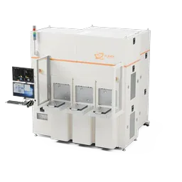
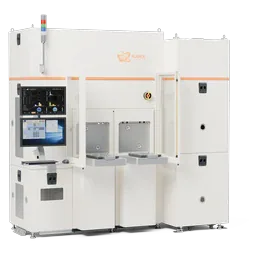
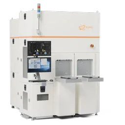
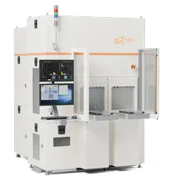
Fully Automatic Patterned Wafer Optical Inspection System Series
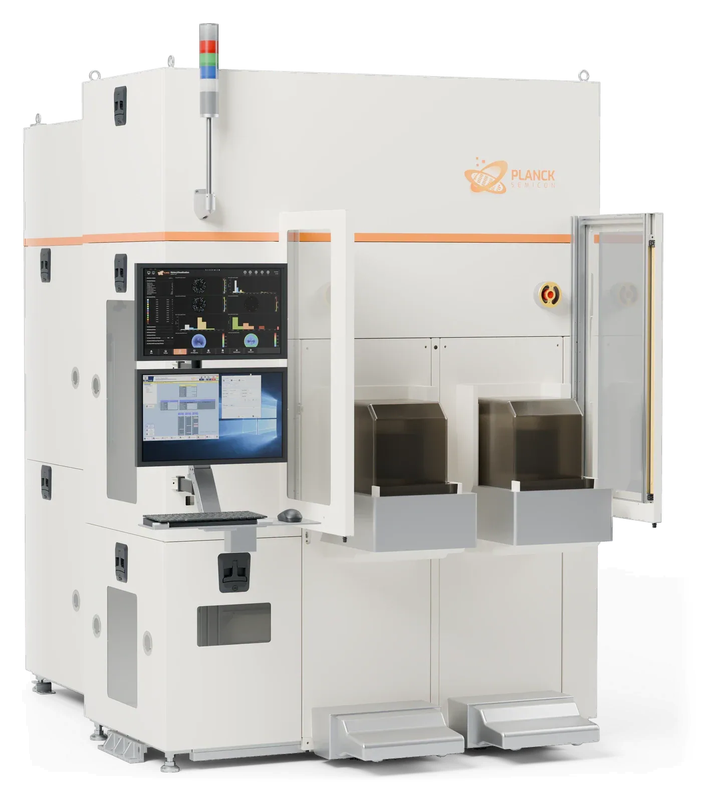
Every side, every wafer, zero compromise
- 2D AOIPattern defects as standard
PAD · Metal lines · RDL and Bump
- 3D AOI · PLOptional capabilities
3D bump inspection for advanced packaging · Organic residue detection
- Wide-fieldIn-house optics for faster scans
Higher throughput at the same resolution
01PRODUCT INTRODUCTION
Overview
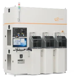
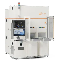
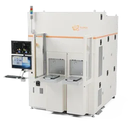
ACONCA is a fully automatic optical inspection series for patterned wafers. In-house wide-field optics with bright-field and dark-field illumination inspect the full wafer. The system detects PAD corrosion, metal residue, foreign material, scratches, edge chipping, photoresist residue, and RDL and bump pattern defects. It classifies defects automatically and outputs a die-level defect map. An optional 3D AOI module inspects advanced-packaging bumps and pillars in three dimensions. An optional PL channel finds organic residue on bumps and PADs that bright-field and dark-field cannot see. Square glass substrates and high-warpage wafers are supported. ACONCA is used in front-end fabs, advanced packaging and 100% inspection of patterned power-device wafers.
Inspection targets
- PAD corrosion
- Metal residue
- Foreign material and scratches
- Edge chipping
- Photoresist residue
- RDL and Bump
- Organic residue by PL
Applications
- Front-end fab process monitoring
- Advanced packaging RDL, Bump and Pillar
- TGV glass substrates
- Patterned power-device wafers
- Pre-bond Bump and PAD residue by PL
02PRODUCT FEATURES
Key features
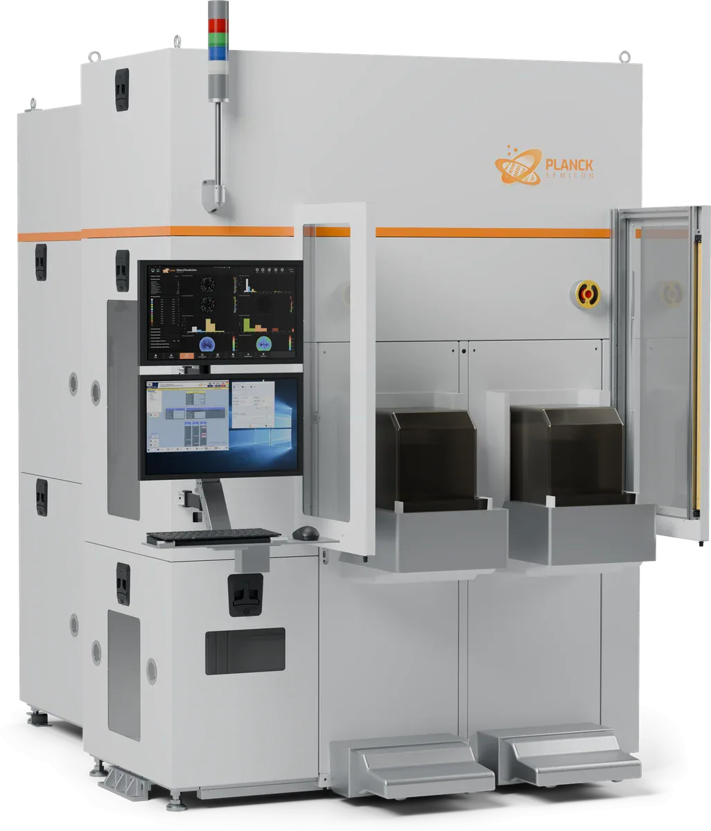
In-house wide-field optics
A larger field of view per frame means less stitching and faster scans at the same resolution
Optional 3D AOI and PL channels
3D AOI inspects advanced-packaging bumps and pillars in three dimensions, and the PL channel detects organic residue on bumps and PADs
Automatic classification and Die Map
ADC classifies defects automatically, and die-level defect maps feed directly into MES / YMS
PLANCKADC · Yield-management ready
Results flow straight into PlanckADC
AI classification and grading, result monitoring with SPC, and Wafer Map traceability, connected to your MES / YMS
About PlanckADC03MORE SYSTEMS
Other systems
- KIBO SeriesUnpatterned Wafer Defect Inspection SystemInspection
- CANIGO SeriesAutomatic Wafer Backside Inspection SystemInspection
- MUSHI SeriesAutomatic Wafer Edge Inspection & Metrology SystemInspection
- CARPPA SeriesFast Inline Process Control SystemInspection
- VEYMONT SeriesFull-Surface Nano-Topography Inspection SystemInspection
- DRAKENS SeriesSiC Wafer Surface & Crystal Defect Inspection SystemInspection
- NANSI SeriesMulti-Channel Wafer Metrology SystemMetrology
- ELBRUS SeriesFull-Wafer Geometry Metrology SystemMetrology
PRODUCT INQUIRY
Discuss yourprocess needs
We match a platform to your material, process step and the parameters you care about
- SalesProducts and commercial inquiriessales@plancksemicon.com
- GeneralCorporate affairs and partnershipsinfo@plancksemicon.com
- Phone
- +86-755-21063549