
Platform series number 05/ 09
INSPECTION SERIES
CARPPA Series
Fast Inline Process Control System Series
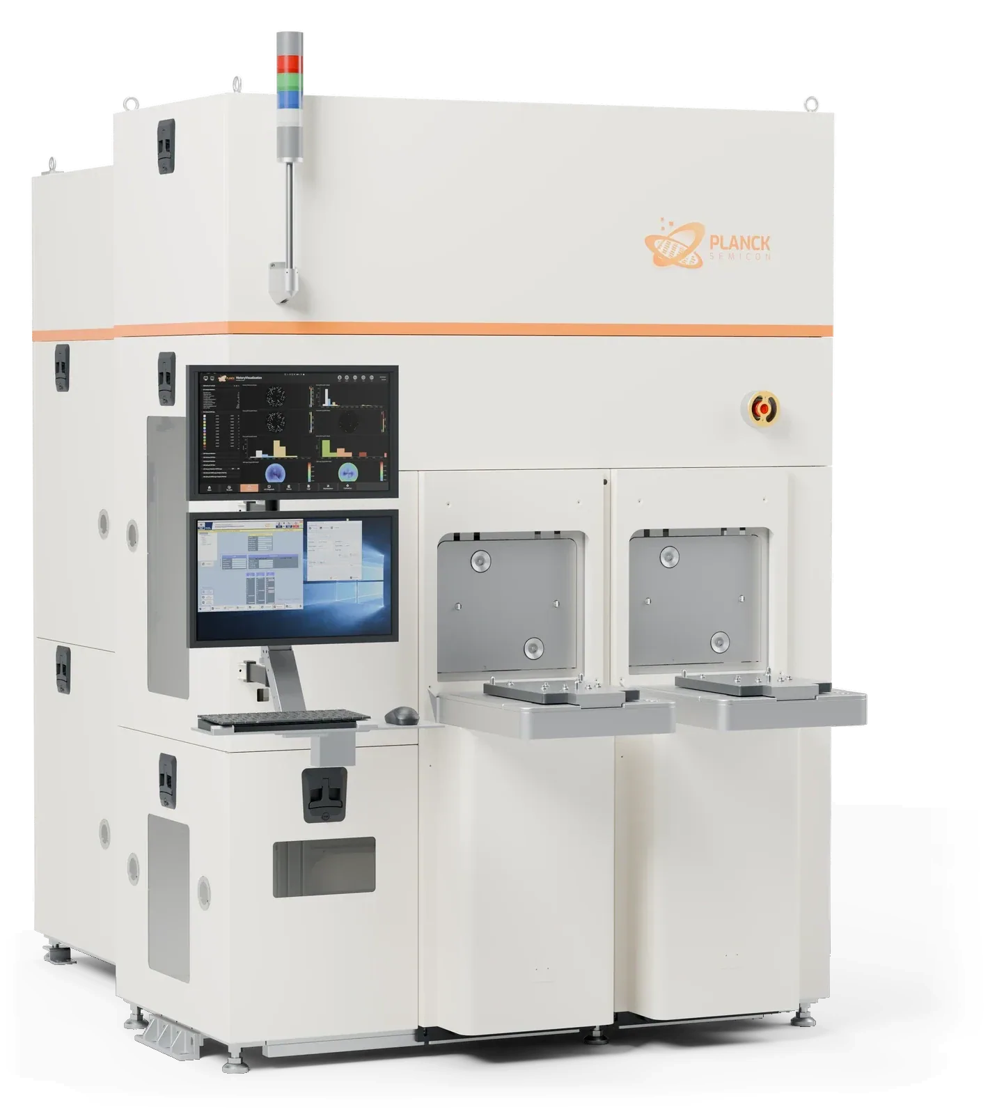
Control at the speed of production
- Recipe-freeReady out of the box
Zero wait for new product introduction
- Fast ADIFast post-litho after-develop inspection
Macro defects · Instant alerts
- 100% inlineInline process-control point
Also after etch, film and CMP
01PRODUCT INTRODUCTION
Overview
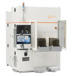
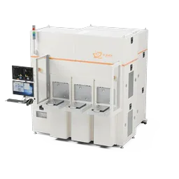
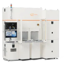
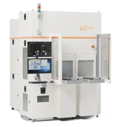
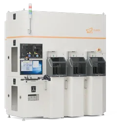
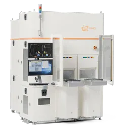
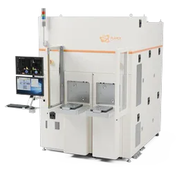
CARPPA is a recipe-free fast macro inspection and process monitoring platform for volume production lines. It is built for Fast ADI, the after-develop inspection that follows lithography. Single-shot full-wafer imaging needs no setup. The system rapidly inspects every wafer for coating non-uniformity, develop defects, comets, bubbles, defocus hotspots and EBR anomalies. It also inspects for macro defects such as scratches, particles and stains. It flags excursions the moment they occur. CARPPA can also be deployed after etch, thin film, CMP and other critical steps as a 100% inspection process-control point.
Inspection targets
- Coating non-uniformity
- Develop defects
- Comets and bubbles
- Defocus hotspots
- EBR anomalies
- Scratches, particles and stains
Applications
- Post-litho ADI
- Front-end volume production
- Film, etch and CMP process monitoring
- Power-device volume production
02PRODUCT FEATURES
Key features
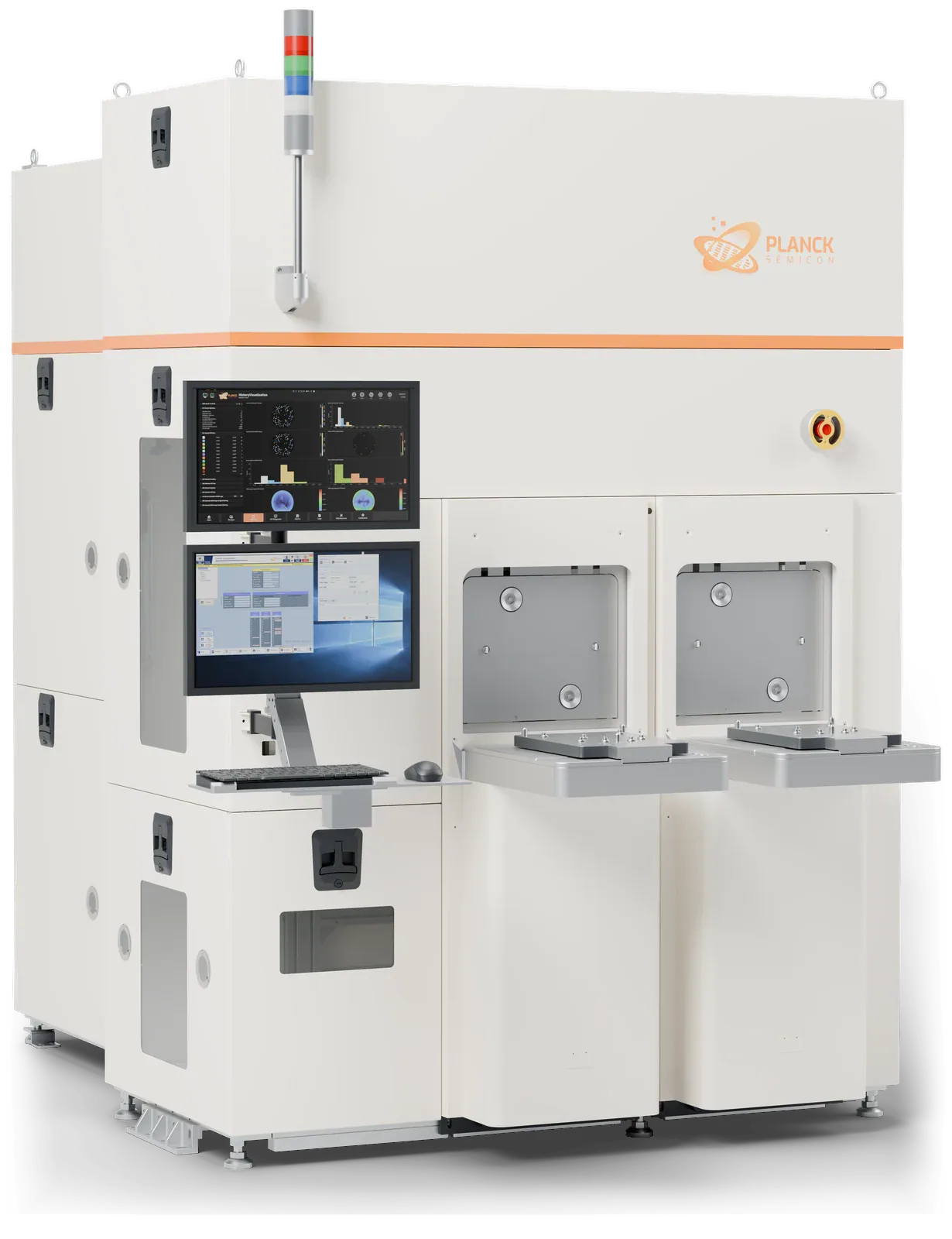
Recipe-free and ready out of the box
No product-specific recipes, no wait for new product introduction, and operator-level ease of use
Fast ADI
Fast full inspection of post-litho develop defects, including coating, develop, focus and EBR anomalies
Real-time alerts and connected data
The system flags excursions the moment they appear and sends SPC trends and alarms to MES / YMS
PLANCKADC · Yield-management ready
Results flow straight into PlanckADC
AI classification and grading, result monitoring with SPC, and Wafer Map traceability, connected to your MES / YMS
About PlanckADC03MORE SYSTEMS
Other systems
- KIBO SeriesUnpatterned Wafer Defect Inspection SystemInspection
- ACONCA SeriesFully Automatic Patterned Wafer Optical Inspection SystemInspection
- CANIGO SeriesAutomatic Wafer Backside Inspection SystemInspection
- MUSHI SeriesAutomatic Wafer Edge Inspection & Metrology SystemInspection
- VEYMONT SeriesFull-Surface Nano-Topography Inspection SystemInspection
- DRAKENS SeriesSiC Wafer Surface & Crystal Defect Inspection SystemInspection
- NANSI SeriesMulti-Channel Wafer Metrology SystemMetrology
- ELBRUS SeriesFull-Wafer Geometry Metrology SystemMetrology
PRODUCT INQUIRY
Discuss yourprocess needs
We match a platform to your material, process step and the parameters you care about
- SalesProducts and commercial inquiriessales@plancksemicon.com
- GeneralCorporate affairs and partnershipsinfo@plancksemicon.com
- Phone
- +86-755-21063549