
Platform series number 06/ 09
INSPECTION SERIES
VEYMONT Series
Full-Surface Nano-Topography Inspection System Series
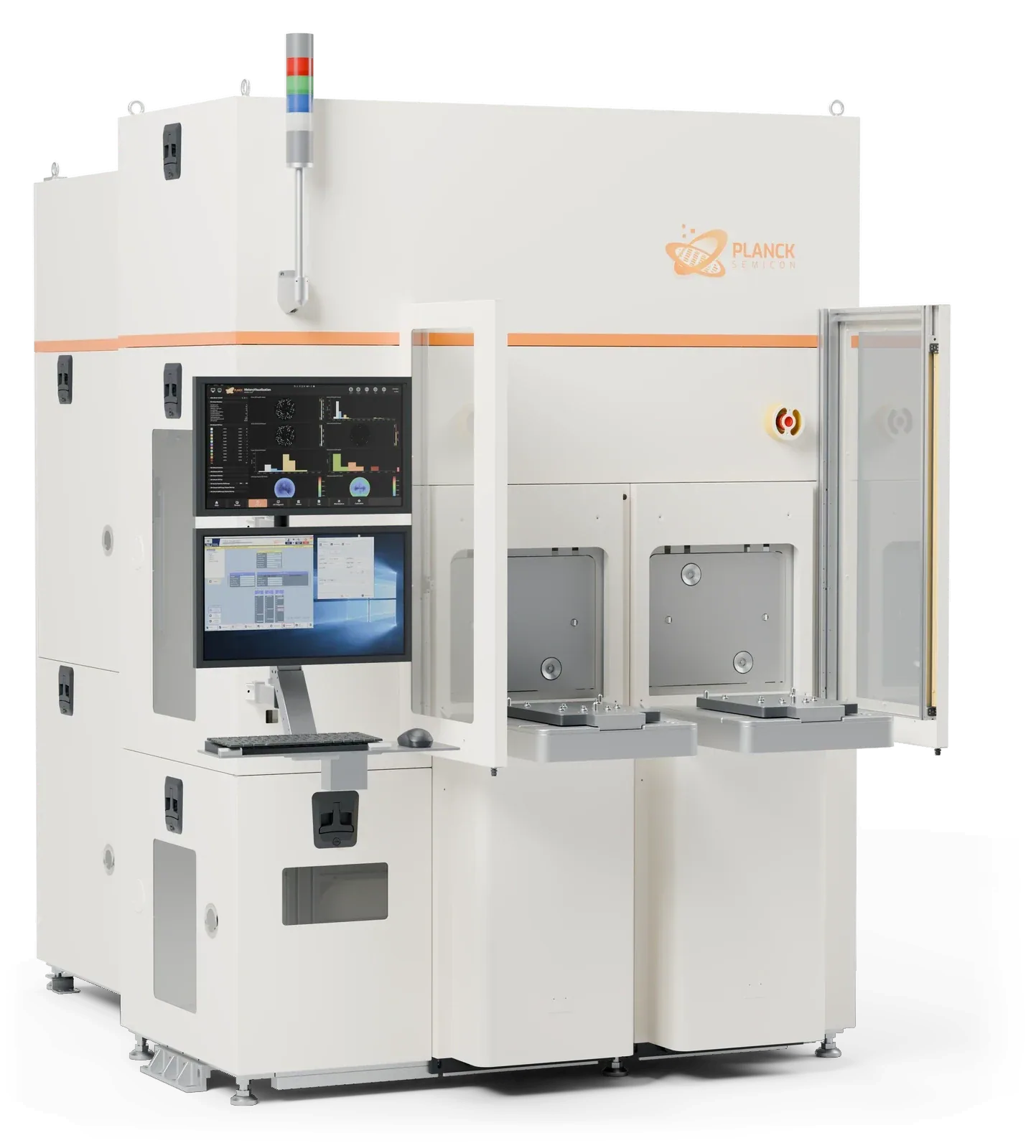
Reveal the invisible
- 2 nmNano-topography · Vertical precision
Dislocation cracks, epi steps, process marks, dimples
- Front + backDual-side simultaneous scan
Single load · Production-rate throughput
- Bonding voidsNon-contact · Can replace CSAM
No couplant · Full wafer in one pass
01PRODUCT INTRODUCTION
Overview
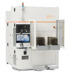
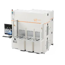
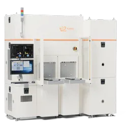
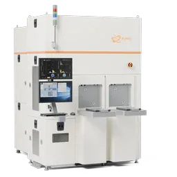
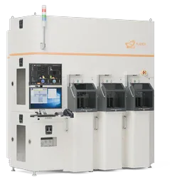
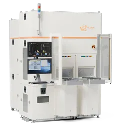
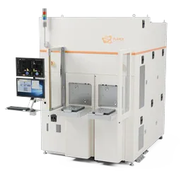
VEYMONT images the entire front and back surfaces of a wafer at nanoscale, with vertical precision down to 2 nm. It reveals dislocation cracks, epitaxial steps, grinding and CMP marks, and local dimples that conventional bright-field and dark-field optics cannot see. It captures substrates and epi wafers completely in a single imaging pass. In advanced packaging, it inspects bonding voids across the full wafer without contact. This can replace CSAM ultrasonic scanning. VEYMONT is used on production lines for silicon wafers, SiC / GaN epi and thinned IGBT backsides.
Inspection targets
- Dislocation cracks
- Epi steps
- Grinding and CMP marks
- Local dimples
- Bonding voids
Applications
- Silicon and SOI wafers
- Hybrid and temporary bonding voids
- SiC / GaN epi
- Thinned IGBT backsides
- CMP process monitoring
02PRODUCT FEATURES
Key features
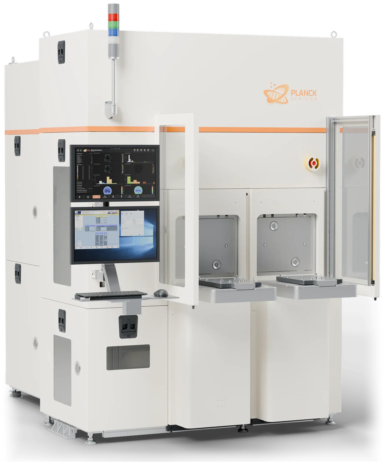
Nano-topography imaging
Dislocation cracks, epitaxial steps, grinding and CMP marks, and local dimples on substrates and epi wafers, captured in a single imaging pass
Non-contact bonding-void inspection
Detects bubbles and voids in hybrid and temporary bonding across the full wafer without couplant, and can replace CSAM ultrasonic scanning
Front and back in one scan
Full dual-side coverage from a single load, with height maps, roughness and local flatness reported together
PLANCKADC · Yield-management ready
Results flow straight into PlanckADC
AI classification and grading, result monitoring with SPC, and Wafer Map traceability, connected to your MES / YMS
About PlanckADC03MORE SYSTEMS
Other systems
- KIBO SeriesUnpatterned Wafer Defect Inspection SystemInspection
- ACONCA SeriesFully Automatic Patterned Wafer Optical Inspection SystemInspection
- CANIGO SeriesAutomatic Wafer Backside Inspection SystemInspection
- MUSHI SeriesAutomatic Wafer Edge Inspection & Metrology SystemInspection
- CARPPA SeriesFast Inline Process Control SystemInspection
- DRAKENS SeriesSiC Wafer Surface & Crystal Defect Inspection SystemInspection
- NANSI SeriesMulti-Channel Wafer Metrology SystemMetrology
- ELBRUS SeriesFull-Wafer Geometry Metrology SystemMetrology
PRODUCT INQUIRY
Discuss yourprocess needs
We match a platform to your material, process step and the parameters you care about
- SalesProducts and commercial inquiriessales@plancksemicon.com
- GeneralCorporate affairs and partnershipsinfo@plancksemicon.com
- Phone
- +86-755-21063549