
Platform series number 04/ 09
INSPECTION SERIES
MUSHI Series
Automatic Wafer Edge Inspection & Metrology System Series
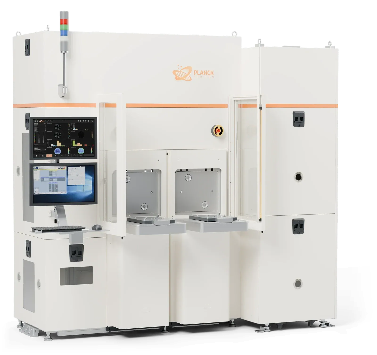
Flawless, right to the edge
- Edge defectsInspection
Chips, cracks, particles, film peeling
- Edge profileMetrology
Upper bevel · Apex · Lower bevel
- All-in-oneInspection and metrology on one tool
Compact footprint · Modular configuration
01PRODUCT INTRODUCTION
Overview
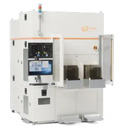
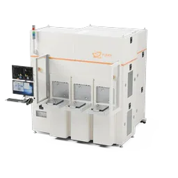
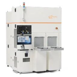
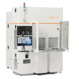
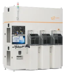
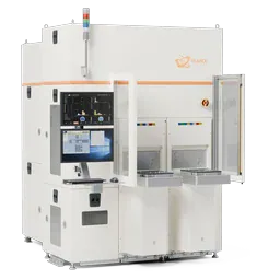
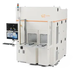
MUSHI is dedicated to the wafer edge. It scans the upper bevel, apex and lower bevel around the full circumference. It detects edge chips, cracks, particles, film peeling and photoresist residue, and measures the edge profile. Inspection and metrology run on the same system. The compact system can be deployed standalone or combined as a module with other inspection functions. It is used for edge control in substrate manufacturing, CMP and thinning, and advanced packaging before bonding.
Inspection targets
- Edge chips
- Cracks
- Particles
- Film peeling
- Photoresist residue
- Edge profile
Applications
- Substrate manufacturing
- CMP and thinning
- Advanced packaging
- Pre-bond edge control
02PRODUCT FEATURES
Key features
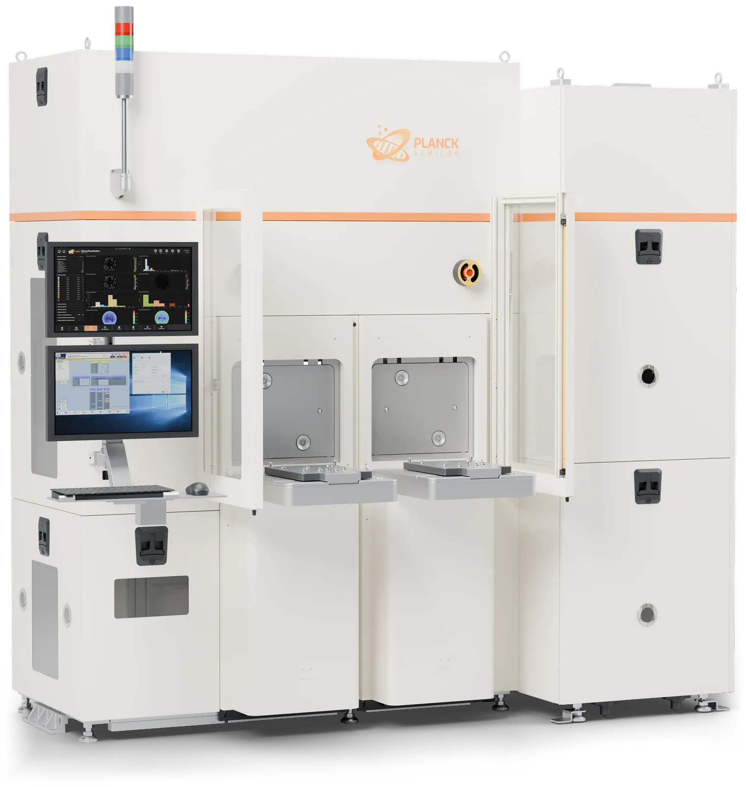
Inspection and metrology in one tool
Edge-defect inspection and edge-profile metrology on the same system
Full-circumference coverage
Upper bevel, apex and lower bevel scanned all the way around, so fine cracks and film peeling are caught early
Compact and scalable
A small footprint, deployable standalone or as a module combined with other inspection functions, built for volume production
PLANCKADC · Yield-management ready
Results flow straight into PlanckADC
AI classification and grading, result monitoring with SPC, and Wafer Map traceability, connected to your MES / YMS
About PlanckADC03MORE SYSTEMS
Other systems
- KIBO SeriesUnpatterned Wafer Defect Inspection SystemInspection
- ACONCA SeriesFully Automatic Patterned Wafer Optical Inspection SystemInspection
- CANIGO SeriesAutomatic Wafer Backside Inspection SystemInspection
- CARPPA SeriesFast Inline Process Control SystemInspection
- VEYMONT SeriesFull-Surface Nano-Topography Inspection SystemInspection
- DRAKENS SeriesSiC Wafer Surface & Crystal Defect Inspection SystemInspection
- NANSI SeriesMulti-Channel Wafer Metrology SystemMetrology
- ELBRUS SeriesFull-Wafer Geometry Metrology SystemMetrology
PRODUCT INQUIRY
Discuss yourprocess needs
We match a platform to your material, process step and the parameters you care about
- SalesProducts and commercial inquiriessales@plancksemicon.com
- GeneralCorporate affairs and partnershipsinfo@plancksemicon.com
- Phone
- +86-755-21063549