
Platform series number 08/ 09
METROLOGY SERIES
NANSI Series
Multi-Channel Wafer Metrology System Series
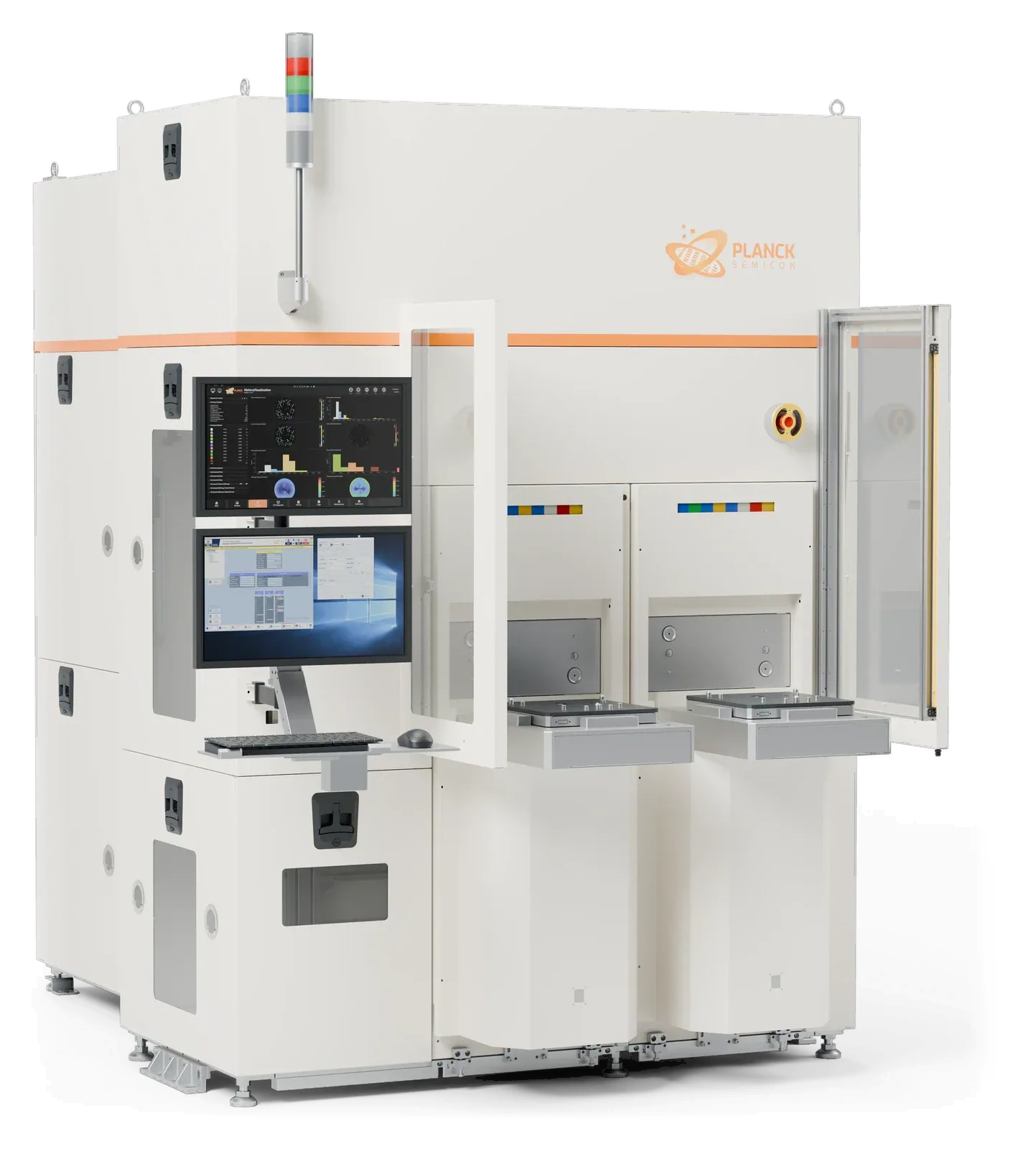
One platform, every measurement
- Front + backSynchronized dual-side probes
Thickness and TTV · Bow / Warp
- Metal layersAccurate on composite stacks
Bonded wafers · Metallized wafers · Per-layer thickness
- Sub-micronMinimum TSV / TGV CD
Deep vias, trenches, high aspect ratio, non-contact
01PRODUCT INTRODUCTION
Overview
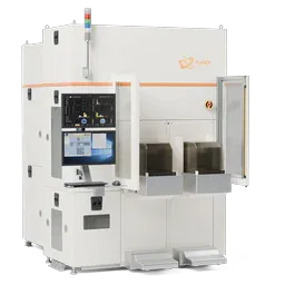
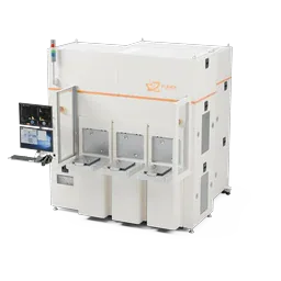
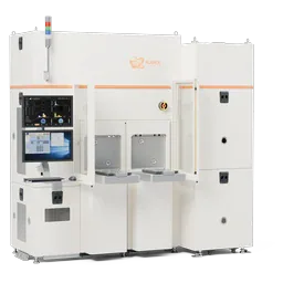
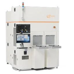
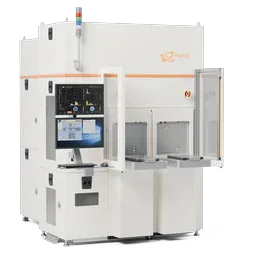
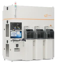
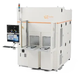
NANSI is a fully non-contact, multi-channel optical metrology platform. Front and back probes measure at the same time. One system measures thickness and TTV, Bow / Warp, film thickness and bonded-stack thickness. It also measures trench depth and CD, TSV / TGV depth and CD, step height and roughness. TSV / TGV CD can be measured down to the sub-micron range. Composite stacks with metal layers are measured just as accurately. NANSI is used in advanced packaging, front-end thinning and CMP, and power-device trenches. It is also used for geometry metrology of silicon and compound substrates.
Measurements
- Thickness and TTV
- Bow / Warp
- Film and stack thickness
- Trench and TSV / TGV
- Step height
- Roughness
Applications
- TSV, bonding and glass substrates in advanced packaging
- Front-end thinning and CMP
- Power-device trenches
- Silicon and SiC substrate geometry
- 3D memory structures
02PRODUCT FEATURES
Key features
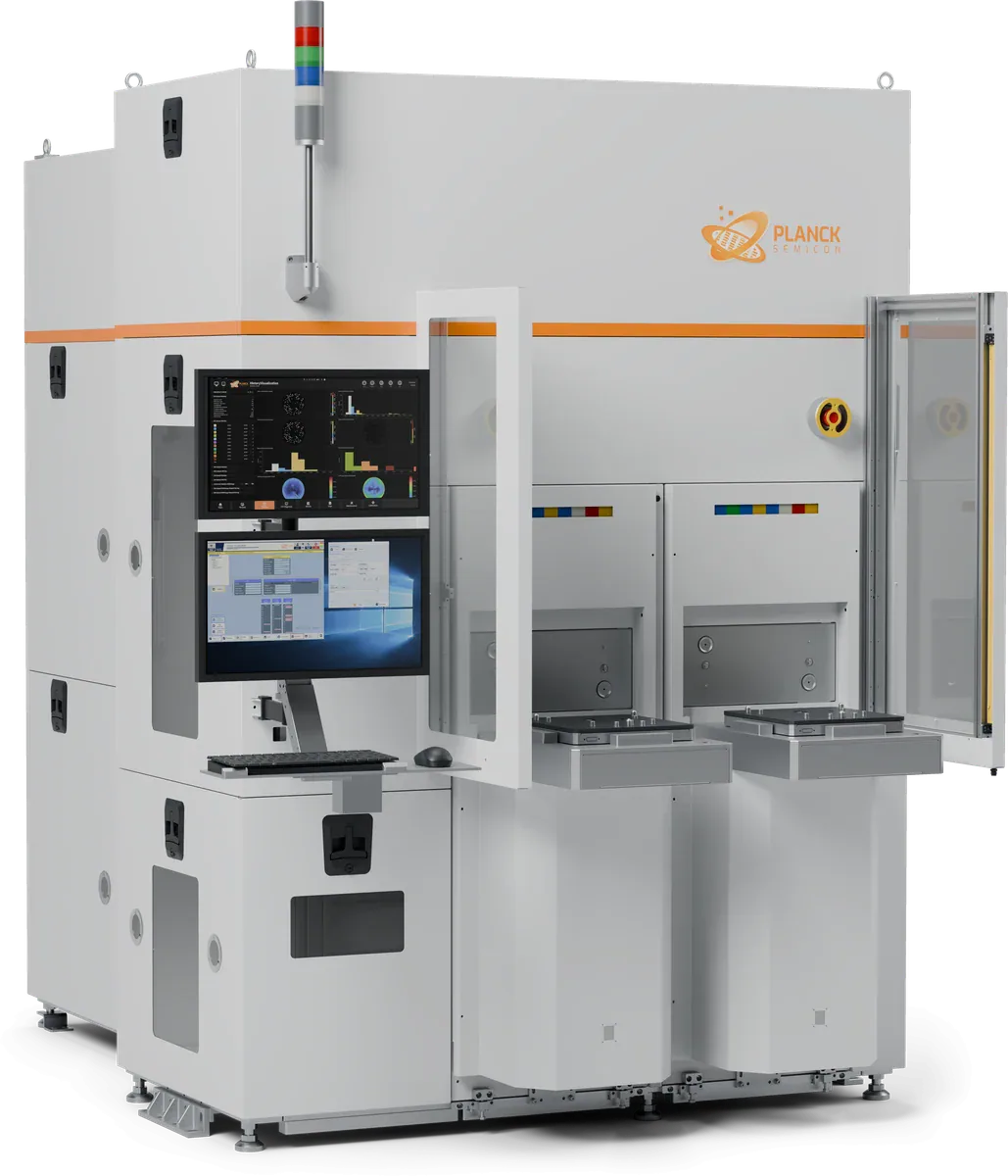
Front and back, measured together
Thickness, TTV, Bow and Warp in a single pass, with gravity compensation
Accurate through metal layers
Every layer of bonded, metallized and other composite stacks measured in one pass
Non-contact via and trench metrology
TSV / TGV CD down to the sub-micron range, with depth and CD of high-aspect-ratio trenches measured without contact
PLANCKADC · Yield-management ready
Results flow straight into PlanckADC
AI classification and grading, result monitoring with SPC, and Wafer Map traceability, connected to your MES / YMS
About PlanckADC03MORE SYSTEMS
Other systems
- KIBO SeriesUnpatterned Wafer Defect Inspection SystemInspection
- ACONCA SeriesFully Automatic Patterned Wafer Optical Inspection SystemInspection
- CANIGO SeriesAutomatic Wafer Backside Inspection SystemInspection
- MUSHI SeriesAutomatic Wafer Edge Inspection & Metrology SystemInspection
- CARPPA SeriesFast Inline Process Control SystemInspection
- VEYMONT SeriesFull-Surface Nano-Topography Inspection SystemInspection
- DRAKENS SeriesSiC Wafer Surface & Crystal Defect Inspection SystemInspection
- ELBRUS SeriesFull-Wafer Geometry Metrology SystemMetrology
PRODUCT INQUIRY
Discuss yourprocess needs
We match a platform to your material, process step and the parameters you care about
- SalesProducts and commercial inquiriessales@plancksemicon.com
- GeneralCorporate affairs and partnershipsinfo@plancksemicon.com
- Phone
- +86-755-21063549